An experiment with HEXFETs.
Page 1 | Page 2 | Page 3 | Page 4
Around Christmas 2005, while completing the P68 subwoofer and advancing on the 1970s-style integrated amplifier, I acquired two valuable books. One was a nifty little little amplifier design guide by G. Randy Slone, and the other was a more detailed (if somewhat arcane) tome by Douglas Self. (Both are referenced in my "resources" section.) As I completed and lightly modified the amplifier circuit in the 1970s-style amp, I was itching to get my hands into the from-scratch approach, when along came the perfect opportunity.
Liam, one of the regular contributors to the Elliott Sound Products forum, posted a possible circuit for a high-power amplifier based around HEXFETs one afternoon. The circuit had simulated well, but never been tested. Reprinted with Liam's permission (click for larger image):

Figure 1. Subwoofer operational diagram. (Click image for a larger view).
I ran a quick tally of the parts cost, assuming use of some BJT devices already on hand, and an expasion
of the FET output stage to six devices per rail, while substituting 0.5Ω source-followers I knew were
available at a nearby surplus shop. No surprises turned up in the numbers, and I decided this might make
for an ideal subwoofer amp.
Generally speaking, vertical MOS is on nobody's short list for quality audio components. HEXFETs are designed for high-current switching, not linear amplification, and the VMOS junctions do not exhibit good linearity until driven at a fairly high (and hot-running) quiescent. Moreover, some of the commonly available and low-cost pairs, notably IRF640 and IRF9640 as used here, are not strictly complementary. In spite of all that, they can be made to perform reasonably well if sufficient heatsinking can be applied, and they are astonishingly robust, with just one exception: susceptibility to strong EMI/RFI interference, since a FET gate is a capacitance-effect device. More on that later.
After toying with some configuration options, I determined that six output devices per rail could be feasibly constructed if I used a daughterboard layout to accommodate the second half of the output stage. The first half and the input stage would live on a motherboard. The daughterboard construction was attempted first:
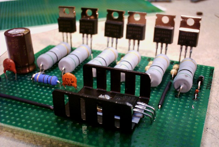
Figure 2. The positive-rail output stage.
Negative rail circuits are sometimes more prone to instability than equivalent positive rail circuits,
all else equal. Whether or not that was an issue here, I did not know. Just to be safe, I built the
positive rail output stage on the daughterboard, and intended to keep the negative rail output stage on
the motherboard, closer to the input stage and global feedback. Six IRF640 devices are present, with
10Ω gate-stopper resistors and 0.5Ω source-followers (5W rated). An MJE15034 predriver
supplies the current to charge the gates. Also visible are the decoupler, a Zobel network, and the
gate-clamping diodes, which can be installed on a FET amp to act as a rudimentary output protection scheme.
This being only a small part of a non-commercial design, I can safely post something that will never
appear in my ESP-based projects: a sample of my protoboard work. Connections are routed with buswire,
generally at right angles, and then soldered. The source-followers dump into a copper strip bus:
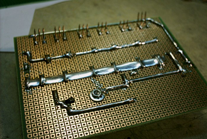
Figure 3. The daughterboard trace and bus routing.
There was also the issue of the heatsink. I found this one at surplus, and figured it would be big enough. The nearly-completed daughterboard is placed on top for comparison:
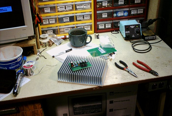
Figure 4. The heatsink, with the daughterboard for reference.
Ayep...that's pretty big. Me like.
Finally, there was the motherboard. It has the input stage:
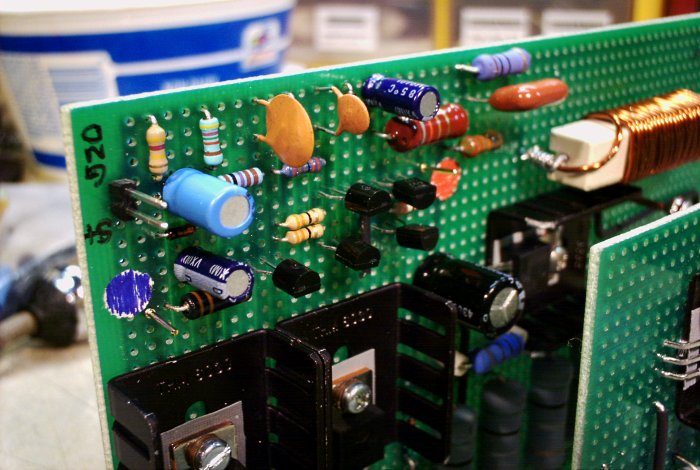
Figure 5. Input stage, located on the motherboard.
It has the voltage amplifier with the thermally-compensated bias servo:
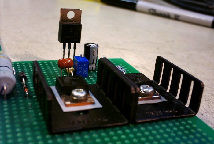
Figure 6. Voltage amplifier stage, located on the motherboard.
And it has the negative-rail output stage, which is constructed identically to the positive-rail stage, but with an MJE15035 for the predriver. Sadly, due to a classic digital editing error, this grainy image is all I have of the overall motherboard prior to assembling it to the daughterboard:
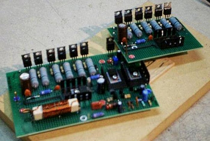
Figure 7. Both boards, ready to be assembled into an amplifier.
The output damper is constructed in the classic DIY fashion: start with a power resistor, then use it as a former
for the parallel output inductor.
With all of that done, it was time to finish assembling the amp and test it.
Optimized for a 1024 viewing width ~//~ All content (c)2008 aaronv.net